Developing Very Small Pixel InGaAs Arrays
Henry Yuan, Jongwoo Kim, Joe Kimchi, Jagmohan Bajaj, Guanghai Ding, James Hwang, Don Lee, William E. Tennant
Teledyne Judson Technologies
Background
Teledyne Judson Technologies (TJT) has been developing InGaAs 2D photodetector arrays designed for very small pixels and large formats. InGaAs is a preferred material for near-infrared and short-wavelength infrared imaging because it combines low dark current, excellent uniformity, mature fabrication technology, and operation near room temperature using thermoelectric cooling. Low-light-level imaging, such as night vision, requires small pixels and extremely low detector noise to achieve sufficient sensitivity. In this context, arrays with 10 to 15 µm pixels are highly desirable, but achieving both small pixel size and large array format presents significant technical challenges.
Challenge
Creating large-format arrays with very small pixels is challenging, because dark current tends to increase as pixel size decreases, primarily due to periphery and surface effects. Maintaining uniformity and low dark current across a full wafer is difficult with conventional fabrication processes. Small pixels require precise control of the p-n junction formation, Zn diffusion, and the cap-absorber interface to prevent shunt and leakage currents. Furthermore, there were very few experimental data available for 10 µm pitch arrays, making it hard to predict performance and optimize design. The performance target for this work was to achieve a dark current density of 0.1 nA cm⁻² or lower at 0 to 7 ºC and a reverse bias of -100 mV.
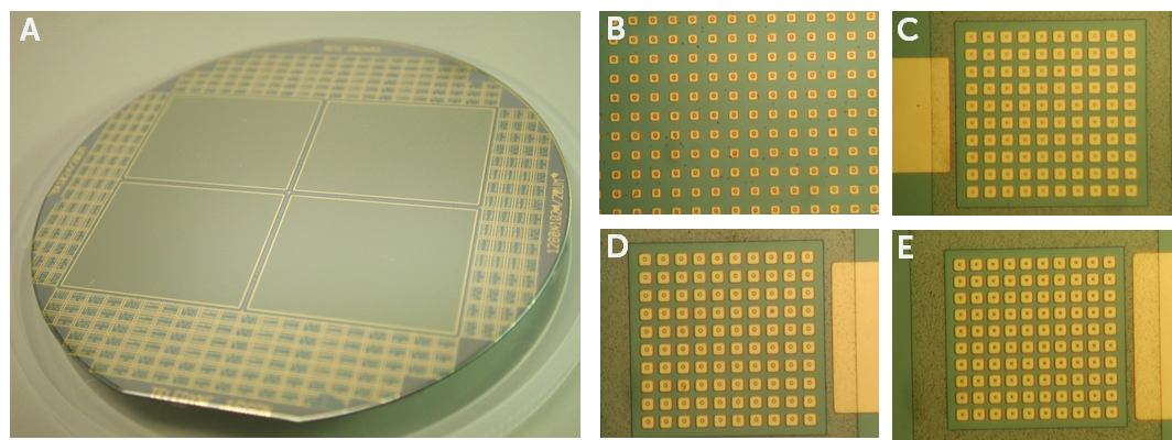
Figure 1: Comparison of pixel arrays on silicon wafers. A) Full 1280x1024 array of 20 µm pixels on a 3 inch wafer, surrounded by test mini-arrays with pixel sizes including 10 µm, 12 µm, 15 µm, 20 µm. B) Magnified view of the 20 µm pixel array seen in A. C) 10 x 10 mini-array of 15 µm pixels. D) 10 x 10 mini-array of 12 µm pixels. E) 10 x 10 mini-array of 10 µm pixels.
Solution
TJT developed a novel all-planar fabrication process suitable for very small pixels and large-format arrays. The team fabricated 10x10 mini-arrays with pixel sizes of 10, 12, 15, and 20 µm alongside 1280x1024 arrays with 20 µm pixels on the same wafer, as seen in Fig.1. The arrays are built on MOCVD-grown In₀.₅₃Ga₀.₄₇As lattice-matched to an InP substrate. Each structure includes an n⁺-InP buffer, an n⁻-InGaAs absorption layer, and an n-InP cap layer, with p⁺ regions formed by Zn diffusion. Indium bumps were deposited to allow connection to silicon read-out integration circuits. For visible-range applications, the InP substrate was removed and a single-layer anti-reflection coating was applied to optimize quantum efficiency.
The arrays were characterized using a cold probe station capable of measuring dark currents down to 1-2 fA over a temperature range from -65 to 200 ºC. The team developed a simplified three-dimensional model to analyze diffusion and generation-recombination currents in small pixels, accounting for periphery effects. Measurements of dark current density versus the pixel perimeter-to-area ratio confirmed that surface and perimeter effects dominate in small pixels. Detector geometry, epitaxial design, and process parameters were optimized to reduce shunt currents and improve effective lifetimes for diffusion and generation-recombination currents.
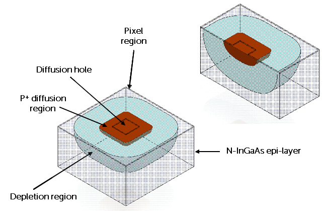
Figure 2: 3D profile and cross-section of a small pixel from a 2D array, where the P+ Zn diffusion region, depletion region, and neutral hole diffusion region are shown in different colors.
Key Performance
For 10 µm pixels in the first wafer fabrication run, the dark current density was 3.2 nA cm⁻² at 7 °C, 1.6 nA cm⁻² at 0 °C, and 0.2 nA cm⁻² at -20 °C at a -100 mV bias. The analysis revealed that excess shunt currents and perimeter effects limit performance, causing dark current to increase as pixel size decreases. The second wafer fabrication run showed a nearly threefold reduction in room-temperature dark current for all pixel sizes. Perimeter-related current was reduced significantly, while bulk current remained largely unchanged. Extrapolations suggest that dark current densities between 0.03 and 0.1 nA cm⁻² are achievable with thermoelectric cooling to -30 to -40 °C.
Conclusion
TJT’s new planar process enables high-performance, very small pixel InGaAs 2D arrays. The 10 µm pixel arrays demonstrate low dark current and high uniformity. Analysis shows that periphery effects dominate the performance of small pixels, and optimization of epitaxial growth, detector geometry, and processing can reduce these effects. The nearly threefold improvement in dark current from the second waferfab run demonstrates the effectiveness of these optimizations. With remaining surface effects addressed, the target of 0.1 nA cm⁻² at 0-7 °C and -100 mV bias is achievable, supporting sensitive low-light-level SWIR imaging in large-format, small-pixel arrays.
Read the original published article(s) here:
Development of Large Format InGaAs 2D Photodetector Arrays with Very Small Pixels
Henry Yuan, Jongwoo Kim, Joe Kimchi, Jagmohan Bajaj, Guanghai Ding, James Hwang, Don Lee, William E. Tennant
Abstract
Teledyne Judson Technologies (TJT) has been developing a novel all planar process suitable for large format very small pixel InGaAs 2D arrays, with the potential for producing <10µm pixels and >2Kx2K format arrays. In this work, a 10µm pixel 2D SWIR array process is successfully demonstrated via the fabrication and testing of 10x10 mini-arrays. A comprehensive cold probing test of dark current was performed at various temperatures and on a series of test array structures with various pixel sizes. For 10µm pixel 10x10 mini-arrays from the 1st waferfab run, test probing showed dark current density of 3.2nA/cm2 at 7ºC and 1.6nA/cm2 at 0ºC, both at -100mV bias. The 10µm pixel dark current data are compared with those from other pixel sizes of 12µm, 15µm, and 20µm. An in-depth analysis of dark current, as a function of bias and temperature, is performed. A simplified 3D modeling is used to simulate the key dark current components such as diffusion current and g-r current while taking into account the perimeter effect for small pixels, and then used to fit the dark current test data. Our work shows that with the optimization of epi-structure and device process designs, as well as the continuing improvement of epi-growth and wafer process quality, it is possible to achieve ≤0.1nA/cm2 dark current density for 10µm pixels in the temperature range of 0- 7ºC and at a reverse bias of -100mV. Further improvement of dark current is achieved from the 2nd waferfab run, with room temperature dark current reduced by almost 3x for all pixel sizes.
Reference
Henry Yuan, Jongwoo Kim, Joe Kimchi, Jagmohan Bajaj, Guanghai Ding, James Hwang, Don Lee, William E. Tennant (17 February 2010) Development of Large Format InGaAs 2D Photodetector Arrays with Very Small Pixels, Proc. SPIE 6950, Laser Radar Technology and Applications XIII, 69500O; https://doi.org/10.1117/12.780363
Recent Progress in Developing Very Small Pixel InGaAs 2D Photodetector Arrays at TJT
Henry Yuan, Joe Kimchi, Louis C. Kilmer, Jonathan T. Getty, Elina R. Glaretas
Abstract
Significant progress has been made at Teledyne Judson Technologies (TJT) in developing technology for ultra low dark current, very small pixel, and large format NIR/SWIR InGaAs photodetector arrays. For 10µm, 12µm, 15µm, and 20µm pixel test arrays, we have achieved the lowest average dark current density of 0.44nA/cm2, 0.44nA/cm2, 0.35nA/cm2, and 0.33nA/cm 2, respectively, at 7ºC and -100mV bias, the best data ever reported so far. This achievement is a significant step towards reaching the goal of ≤0.1nA/cm2 for 10µm pixels. Furthermore, TJT is now developing technology for sub-10µm pixel arrays, and has successfully demonstrated, for the first time, the feasibility of making 5µm pixel test arrays. Our preliminary results showed very promising performance, achieving the average dark current density of 28.6nA/cm2 for 5µm pixels, 25.2nA/cm2 for 6µm pixels, and 20.2nA/cm2 for 8µm pixels at 23ºC and - 100mV bias. Comprehensive dark current characterization and data analysis are presented in this paper. Finally, in collaboration with Raytheon Vision Systems (RVS), high performance Vis-InGaAs 640x512/20µm FPAs have been developed, using a substrate removed structure which extends the spectral response to UV-visible wavelength range.
Low dark current small pixel large format InGaAs 2D photodetector array development at Teledyne Judson Technologies
Henry Yuan, Mike Meixell, Jiawen Zhang, Philip Bey, Joe Kimchi, Louis C. Kilmer
Abstract
Teledyne Judson Technologies (TJT) has been developing technology for small pixel, large format, low dark current, and low capacitance NIR/SWIR InGaAs detector arrays, aiming to produce <10µm pixels and >2Kx2K format arrays that can be operated at or near room temperature. Furthermore, TJT is now developing technology for sub-10µm pixel arrays in response to requirements for a variety of low light level (LLL) imaging applications. In this paper, we will review test data that demonstrates lower dark current density for 10-20µm pixel arrays. We will present preliminary results on the successful fabrication of test arrays with pixels as small as 5µm. In addition, a lot of effort has been made to control and reduce the detector pixel capacitance which can become another source of detector noise. TJT is also developing 4” InGaAs wafer process and now offers four different types of InGaAs 2D arrays/FPAs that are tailored to different customer requirements for dark current, capacitance, spectral response, and bias range.
Reference
Henry Yuan, Mike Meixell, Jiawen Zhang, Philip Bey, Joe Kimchi, and Louis C. Kilmer (31 May 2012) Low dark current small pixel large format InGaAs 2D photodetector array development at Teledyne Judson Technologies, Proc. SPIE 8353, Infrared Technology and Applications XXXVIII, 835309; https://doi.org/10.1117/12.921232