Advancing InAs Photodetectors with Mesa Etch and Surface Passivation Technologies
Vicky W. Zhang, Jongwoo Kim, Henry Yuan, John Clark, Mike R. Meixell, Carl Meyer, Witold Czelen, Eli Sullivan, Gary Apgar, Jeremy Palmer, Joyce Laquindanum, Ravi Guntupalli
Teledyne Judson Technologies
Background
Indium arsenide (InAs) is a highly attractive semiconductor material for mid-wavelength infrared (MWIR) photodetectors due to its narrow bandgap and very high near-surface electron mobility. It is widely used in high-performance transistors, optical devices, chemical sensors, type-II superlattice detectors, and avalanche photodiode arrays. Despite these advantages, the lack of a reliable and stable surface passivation process has long limited the performance and reliability of InAs photodetectors.
Native oxides on InAs surfaces are unstable and degrade over time, releasing indium and arsenic species that can compromise device stability and pose additional challenges in sensitive applications such as biological sensing. This unstable oxide layer introduces high defect densities, which degrade key detector parameters including dark current, shunt resistance, and breakdown voltage. Previous attempts at surface passivation often resulted in degraded device performance, leaky junctions, or poor long-term stability, particularly after packaging and thermal cycling. For these reasons, Teledyne Judson Technologies (TJT) historically manufactured InAs photodetectors without any passivation layer, accepting certain limitations in performance and stability.
Challenge
The primary challenge in developing a stable surface passivation for InAs photodetectors lies in controlling the highly leaky InAs–dielectric interface and preventing degradation of device performance. Traditional passivation methods, including wet chemical treatments, dielectric deposition, and encapsulation techniques, often introduce surface states or mechanical stress that lead to increased leakage currents and reduced shunt resistance.
Even when acceptable electrical performance was achieved at the wafer level, many devices exhibited instability during subsequent assembly and packaging processes, with degraded dark current, reduced breakdown voltage, or drifting shunt resistance over time. This instability was further complicated by the need for compatibility with standard fabrication flows and packaging steps, as well as the desire for passivation layers that could simultaneously function as anti-reflection coatings (ARC) to enhance quantum efficiency (QE).
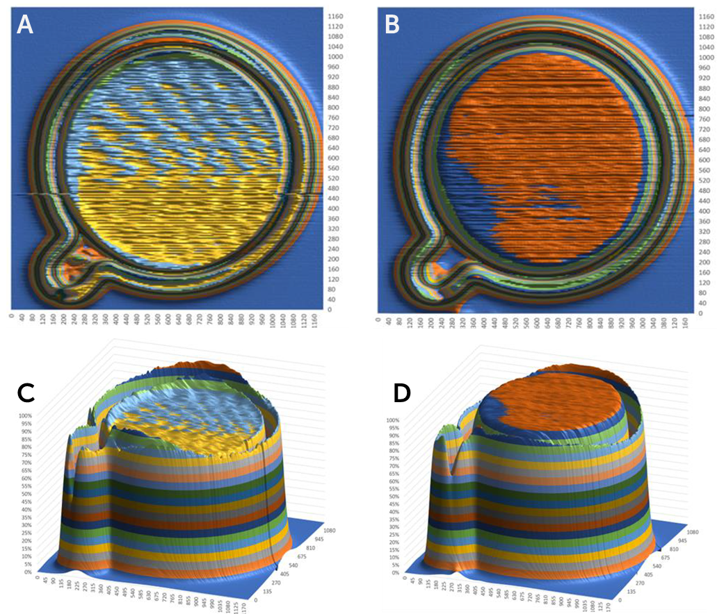
Figure 1: Visualisation of the passivation effect, comparing non-optimised with optimised passivation thicknesses at -65 °C. A) Top view raster scan of a non-optimised diode. B) Top view raster scan of an optimised diode. C) 3D view of raster scan from A. D) 3D view of raster scan from B.
Solution
TJT has developed a new surface passivation process tailored for InAs mesa photodetectors that overcomes these historical limitations. The solution involved optimising every stage of device fabrication, including mesa etching, surface treatment, passivation material selection, and deposition conditions. Multiple passivation approaches such as wet chemical cleaning, polymer encapsulation, atomic layer deposition (ALD), and thermal evaporation were systematically evaluated through a design-of-experiments (DOE) approach.
Key process parameters such as mesa height, junction depth, coating thickness, and film stress were studied and tuned to minimise interface defects and leakage paths. The resulting passivation process was carefully integrated into the existing fabrication flow to ensure compatibility with downstream packaging and assembly. Importantly, the passivation layer was designed to act as an ARC optimised near 2.7 µm, significantly enhancing spectral response and QE without introducing new interface defects.
Results
The introduction of the new passivation process led to substantial improvements in both the optical and electrical performance of InAs photodetectors. Shunt resistance increased significantly, even after full device packaging, and dark current remained low and stable across a wide temperature range. Measurements demonstrated that key electrical parameters such as breakdown voltage and series resistance were unaffected or improved after passivation, indicating a well-controlled and stable surface interface.
Optical performance also improved markedly. Passivated detectors exhibited higher responsivity and a broader spectral response compared to non-passivated devices, with responsivity increases exceeding 50% at room temperature. When optimised for ARC performance, the passivation layer reduced surface reflection from over 30% to below 5% across the 1.5-3.5 µm range, further enhancing QE.
Temperature-dependent measurements confirmed excellent performance stability down to -65 °C, with more than 20% higher responsivity compared to unpassivated devices. Passivation also improved spatial uniformity: raster and focused spot scans revealed over 95% responsivity uniformity across the active detector area, with less than 5% variation. Furthermore, process refinements reduced coating thickness non-uniformity from more than 20% to just over 1%, ensuring highly repeatable performance across production wafers.
Conclusion
The development of a robust surface passivation process for InAs mesa photodetectors represents a major advancement in device performance, reliability, and manufacturability. TJT’s new approach eliminates many of the limitations historically associated with InAs surface treatment, delivering devices with stable electrical behaviour, significantly improved responsivity, and enhanced optical performance.
In addition to stabilising the detector interface and improving yield, the passivation layer serves as an effective ARC, providing further gains in quantum efficiency. With these advances, InAs photodetectors now exhibit excellent stability and performance over a broad temperature range, making them highly suitable for demanding MWIR applications. This work establishes a foundation for future InAs-based device designs and opens the door to improved photodiode arrays, sensors, and imaging systems with superior performance and reliability.
Read the original published article here:
MESA etch and surface passivation for InAs photodetectors: optical, electrical performance, and stability improvement
Vicky W. Zhang, Jongwoo Kim, Henry Yuan, John Clark, Mike R. Meixell, Carl Meyer, Witold Czelen, Eli Sullivan, Gary Apgar, Jeremy Palmer, Joyce Laquindanum, Ravi Guntupalli
Abstract
InAs is a very attractive material for high performance transistors, optical applications, and chemical sensing. However, it has been very challenging to achieve high stability surface passivation layer over InAs due to the very high leaky InAs and passivation interface. Various passivation method attempts in the past were not successful at TJT as they all caused significant degradation of InAs detector performance. As a result, no surface passivation has been used for TJT standard InAs photodetectors until now.
In this paper, we report for the first time a successful development of a new surface passivation process that is suitable for TJT InAs mesa photodetectors. This passivation did not cause InAs detector performance degradation and showed good stability and process compatibility with the detector assembly/packaging processes. Etching methods have been evaluated and applied to form InAs mesa photodiodes. Afterwards, multiple paths for surface treatment and passivation, including wet treatment, Polymer Encapsulation, Atomic Layer Deposition and Thermal Evaporation, have been compared and applied to the as developed photodiodes. Extensive characterization on InAs mesa and passivation quality were then performed. Key control factors, including surface treatment, mesa height, junction depth, etc., have been studied and optimized through design of experiment (DOE). Optical and electrical characterizations of detector performance have been performed and analyzed, including dark current, capacitance, shunt resistance, spectral responsivity and QE, and spatial uniformity over various temperatures. By optimization of passivation process, the significantly improved device performance stability has been achieved and presented in this paper. In addition, the new surface passivation layer also serves as an anti-reflection coating (ARC) that enhances the InAs detector spectral response and QE when optimized to the wavelength of interest.
Reference
Vicky W. Zhang, Jongwoo Kim, Henry Yuan, John Clark, Mike R. Meixell, Carl Meyer, Witold Czelen, Eli Sullivan, Gary Apgar, Jeremy Palmer, Joyce Laquindanum, and Ravi Guntupalli (2024) MESA etch and surface passivation for InAs photodetectors: optical, electrical performance, and stability improvement, Proc. SPIE 13046, Infrared Technology and Applications L, 130461D; https://doi.org/10.1117/12.3021053