Large area, High Speed InGaAs Detectors
Henry Yuan, Jongwoo Kim, Gary Apgar, Joyce Laquindanum, Kai Song, Joseph Kimchi, Ted Wong
Teledyne Judson Technologies
Background
InGaAs photodiodes are the workhorse detectors for near-infrared (NIR) sensing, operating effectively across the 0.9-1.7 µm wavelength range. They are critical components in a wide variety of applications, including laser range finding, pulsed detection, LIDAR, laser warning and tracking systems, and precision alignment. Many of these use cases demand photodetectors with large active areas, often greater than 3 mm in diameter, and response times in the nanosecond regime. However, conventional InGaAs PIN photodiodes struggle to meet these requirements due to high junction capacitance, which limits their speed.
Teledyne Judson Technologies (TJT) has developed a new class of large-area, high-speed InGaAs photodetectors based on a novel thick, fully depleted PIN architecture. These devices offer dramatically reduced capacitance and faster response times while maintaining excellent dark current, breakdown voltage, and spectral performance comparable to standard devices.
Challenge
The performance of a PIN photodiode in high-speed applications is typically limited by three key factors: carrier transit time across the depletion region, diffusion time outside the depletion region, and the resistance-capacitance (RC) time constant determined by the junction capacitance and load resistance. For large-area detectors, the RC time constant dominates. Because capacitance is inversely proportional to the intrinsic layer thickness, increasing that thickness is the most effective way to reduce capacitance and speed up response.
However, growing a significantly thicker InGaAs intrinsic layer without compromising material quality, uniformity, or electrical characteristics is challenging. It requires precise epitaxial growth and careful control of background doping levels to achieve full depletion at practical reverse bias voltages.
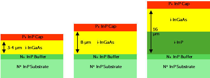
Figure 1: Comparison of traditional InGaAs PIN structure to the very thick PIN structures with single or dual depletion region: (left) standard PIN, (mid) 8 µm PIN, and (right) 16 µm dual-depletion region PIN.
Solution
TJT has engineered a new generation of large-area InGaAs photodetectors with intrinsic layers two to four times thicker than those in conventional designs. Two advanced device architectures have been realized, as shown in Fig.1. The first is an 8 µm PIN design, which increases the i-layer thickness from the typical 3–4 µm to 8 µm. The second is a 16 µm dual-depletion region (DDR) PIN, which combines intrinsic InGaAs and InP layers to achieve a total depletion thickness of 16 µm. Both structures achieve dramatic reductions in junction capacitance (by factors of 2 to 4) resulting in much shorter RC-limited response times.
These detectors are available in both frontside-illuminated and backside-illuminated configurations (shown in Fig.2), with both versions demonstrating excellent spectral response, spatial uniformity, and thermal stability. Despite the thicker structure and larger active area, the new devices maintain low dark current levels (on the order of a few nanoamps at typical operating voltages) and high breakdown voltages above 15-20 V, comparable to conventional photodiodes.
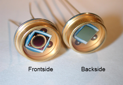
Figure 2: Photo of 3.5mm diameter HS InGaAs PDs in TO-8 package: frontside vs. backside illumination
Performance and Characterisation
Electro-optical characterization of these detectors demonstrates significant performance gains. Capacitance-voltage measurements show that the 8 µm PIN achieves a capacitance of approximately 165 pF at -10 V, roughly half that of a conventional PIN, while the 16 µm DDR device achieves about 100 pF at -40 V, representing a more than threefold reduction. This translates directly to faster response times, with the RC-limited rise time dropping from about 37 ns for a standard PIN to 17 ns for the 8 µm device and 11 ns for the 16 µm DDR structure.
Dark current measurements confirm that performance remains stable despite the structural changes. Both device types exhibit dark currents ranging from a few nanoamps to about 20 nA at reverse biases up to 15–20 V, with breakdown voltages typically near 20 V. Temperature-dependent testing shows predictable behavior across a wide temperature range, with diffusion current dominating near room temperature and generation-recombination current at lower temperatures. Even under elevated operating conditions, the detectors show consistent and well-behaved characteristics.
Spectral measurements demonstrate high responsivity and quantum efficiency. Both device types deliver typical responsivity around 0.6-0.7 A/W at 1.0 µm and 1.0-1.1 A/W at 1.5-1.6 µm. Quantum efficiency reaches 80-90% for the 8 µm PIN and 75-85% for the 16 µm DDR PIN in the 1.0-1.6 µm range. Temperature-dependent spectral data show minimal degradation and predictable shifts in cutoff wavelengths due to bandgap changes, while backside illumination performance can be extended into the visible range by substrate removal.
The detectors also exhibit excellent linearity and uniformity. Photoresponse remains linear beyond 100 mW for backside-illuminated devices and up to 25-40 mW for frontside-illuminated devices, with responsivity near 1 A/W. Spatial response uniformity is better than 2% across the full 3.5 mm active area, confirming high-quality epitaxial growth and fabrication processes.
|
Parameter |
Conventional PIN |
8 µm PIN |
16 µm DDR PIN |
|
Intrinsic layer thickness |
3–4 µm |
8 µm |
16 µm |
|
Capacitance (Cd) |
~340 pF |
~165 pF |
~100 pF |
|
RC rise time (τr) |
~37 ns |
~17 ns |
~11 ns |
|
Dark current (Id) |
Few nA – 20 nA |
Few nA – 20 nA |
Few nA – 20 nA |
|
Breakdown voltage (Vbr) |
~15–20 V |
~17–20 V |
~20–22 V |
|
Quantum efficiency (QE) |
~80–90% |
80–90% |
75–85% |
|
Uniformity |
<2% variation |
<2% variation |
<2% variation |
Future Development
Further optimization of background doping in the intrinsic layers, particularly the InP layer in the DDR structure, could enable even lower capacitance values (<80 pF) and improved reach-through at lower bias voltages. Additionally, the technology platform demonstrated here can be scaled to even larger active areas (5, 10, or 15 mm diameter) while preserving the same low-capacitance, high-speed performance.
Conclusion
Teledyne Judson Technologies’ large-area, high-speed InGaAs photodetectors represent a major advancement in PIN photodiode design. By reengineering the intrinsic region and introducing dual-depletion architectures, these devices achieve significantly reduced capacitance and more than threefold improvements in response time, all while maintaining low dark current, high breakdown voltage, excellent quantum efficiency, and exceptional uniformity.
These detectors are ideal for next-generation high-speed applications, including LIDAR, laser warning and tracking, pulsed detection, and precision optical measurement systems. The demonstrated technology provides a scalable path forward for even larger detector sizes and more demanding system requirements.
Read the original published article here:
Large-area high-speed InGaAs photodetectors
Henry Yuan, Jongwoo Kim, Gary Apgar, Joyce Laquindanum, Kai Song, Joseph Kimchi, Ted Wong
Abstract
A novel InGaAs structure has been developed specifically for use in high-speed applications that require large active area diodes with greater than 3mm diameter size. The device design is based on a thick and fully depleted PIN structure. The intrinsic layer thickness is 2 to 4 times thicker than that of the conventional PIN detectors. Greater than 3-fold reduction in detector capacitance per unit area and the corresponding RC time constant has been demonstrated. Even with such significant speed enhancement, other diode performance characteristics such as dark current and breakdown voltage of these novel InGaAs PIN detectors remain comparable to those of the conventional structure. Front- and backside-illuminated InGaAs detectors are fabricated. Both show equally high-quality spectral response and spatial uniformity. Comprehensive electro-optical tests are performed and the data and analysis are presented. Temperature dependent performance characteristics are also reported. Well-behaved performance characteristics are observed from TE-cooled temperatures to elevated temperatures above ambient.
Reference
Henry Yuan, Jongwoo Kim, Gary Apgar, Joyce Laquindanum, Kai Song, Joseph Kimchi, and Ted Wong (16 April 2008) Large-area high-speed InGaAs photodetectors, Proc. SPIE 6950, Laser Radar Technology and Applications XIII, 69500O; https://doi.org/10.1117/12.780363